IIT Kanpur Interview Experience -  Microelectronics, VLSI & Display Technologies (2014)

IIT Kanpur Interview Experience - Microelectronics, VLSI & Display Technologies (2014)


This is the interview experience of Disha Shrivastava,which i had read  while looking for details on IIT Kanpur on her personal blog .
YEAR- 2014  (GATE ECE)
The list of shortlisted candidates for IIT Kanpur MTech interview was put up on the website. I had applied in three specializations at IIT Kanpur : 1) Microelectronics, VLSI & Display Technologies 2) Signal Processing & Communication 3) RF & Microwave in the same order of preference, but my name was appearing in only one list ( VLSI ) though my GATE score was above the cutoff in other two specializations as well. This outcome puzzled me and then I came to know the hard truth which was not revealed to me either by IIT Kanpur or anyone else while applying. At IIT Kanpur, they will shortlist you only for one specialization based on your order of preference and will interview you only in that specialization. You can’t even appear for the interview of other specializations even if your score is higher than its cutoff. So, friends be very careful while applying. Give preferences based both on your interests and the areas which you are strong in so that you can display your worth in the interviews.

I had stayed in IIT Kanpur for two months as part of my summer project after BE 2nd year. So, I was very much aware of the campus and the locations of each department. They had marked two days for the interview (6th – 7th May) which seemed justified when I entered a huge hall packed with students on 6th at 7 am. They had called around 350 students for interview of just one specialization ( VLSI )!! After 2-3 hours of confusion among the co-ordinators and growing impatience of the students, interviews were finally started. We were dispatched from the lecture hall in groups of 10 students to reach the Electrical Engg. Dept where interviews were being held. I learnt from the co-ordinators that there were 3 interview panels for VLSI each consisting of 2-3 professors.There was no fixed sequence of sending students inside. Everyone in the room had to catch a train at night and so order was changed based on their convenience ( Many people creating fake flights and trains). My name was 3rd in the list but thanks to our urgency friends, I was dropped down to 18th spot. In store for me were, yes you guessed it right a decade of waiting hours😦  To add to my irritation, profs. were conducting a single interview for 50-55 mins..Being tired both mentally and physically, finally my chance came at 7pm.
Interview:
There were two professors in my Panel. As soon as I entered the room they handled me a chalk and sent me to the blackboard adding to my anxiety. The questions which they asked were as follows:
  • Draw the drain current vs gate-to-source voltage curve for nMOS.
  • Write the equation for drain current ( asked what each parameter is in the equation)
  • What is mobility? Draw its graph showing its variation with temperature. Why does it show such a dependence. Explain.
  • Draw the circuit of a CMOS inverter. Justify the connections (i.e, why nmos substrate is connected to ground,etc.)
  • Draw Voltage Transfer Curve ( VTC ) of CMOS. How will the VTC change if pmos is replaced with a resistance.
  • What is switching threshold voltage? Derive an expression for it. How does it depend on W/L ratio?
  • Draw the VTC if W/L ratio of pmos is increased/decreased.
The interview lasted for about 45 mins. I answered 85% of the questions and they were satisfied with my explanations. Some of the questions were not of undergraduate level and they themselves said that they were not expecting me to answer them. Learning from my earlier mistake, I had studied some analog and devices portion before reaching Kanpur. At the end of the interview, I was quite happy with my performance (especially compared to previous one) and was relieved that now I can go home. I heard that all the interviews after me ( that day and the next day) were just 10-15 mins long ; so luck also favoured me in a way here. The results were out quite late ( May End) and I was selected with 36 other people:) ( Note: The intake at VLSI at iitk is roughly 12-13 ; but since they release only one list, they have to keep margin and thus make offer to more candidates).
Pros:
  • IIT Kanpur is known for its academics and is also quite reputed for being a good research institute (some say it is the 2nd best after IISc in research).
  • IITk mess offers the best food you can have in any of the IIT’s and IISc. The quality and the variety of food is pretty good. The act of hot rotis being served as soon as you finish the one on your plate and drinking water being changed periodically to ensure that it remains cold happens only in Kanpur J
  •  The campus is beautiful and very well maintained (as soon as a leaf falls on the road, it is swept off immediately ); good hostels with 24 hours functioning canteens; amazing playgrounds for almost all sports and dancing peacocks provide irresistible attractions:)
  • One thing which I liked very much and which I would like to mention is the attitude of the mess staff and security guards. They take care of you as a child and are always ready to help in a sincere and polite way.
Cons:
  • Apparently, the best specialization for EC at IITk is not Microelectronics & VLSI , its Signal Processing & Communication (I came to know about this later and this was one of the mistakes which I made while applying ) It is good both for research and placements. Surprisingly, the cut-off for Spcom was much lower than VLSI and its intake was also huge (70).
  • The academic system at iitk is quite stringent in the sense that you get only even grades (after 10 comes 8 then 6 ;which means there are no 9’s and 7’s). This affects your CGPA and can be a concerning factor if you are applying for PhD abroad.
  • According to the current batch students studying VLSI there, the faculty members in this course are very less and 90% of the research going on is in the field of Devices (which sadly doesn’t have much scope in India till now; but has wide opportunities abroad).To add to the grievances, were the below average placements in VLSI this year (This doesn’t mean that placements are always like this)

Integrated Electronic Circuits Interview Experience (IIT-Delhi)


VDTT+IEC = VLSI of IIT-D


This is the interview experience of my friend Himanshu Lohani, who secured AIR 88 with a Gate score of 879 in GATE 2016 ECE at IIT Delhi conducted on May 17 & 18.

VDTT is a completely sponsored course. It comprises of three stream CSE +EE +EC. There is no reservation in this, only course in Delhi without reservation with intake of around10 students. Some employees are sponsored by their companies and gate freshers qualified are to be sponsored from industries Texas, Cadence, Cypress and internal project.

Gate cutoff score for both course was 800. As my gate score is 879, AIR-88. I was shortlisted for both.


VDTT 1st Round

I didn’t crack first round which is professor round. Here I am giving my experience. There were total 91 candidates called for VDTT I had seen the list during document verification, out 10 were from CSE, 61 from EC and 20 from EE. Many candidates were absent that day. There were total 5 to 6 panels, 3 are for EC and for rest 1 each.

The Asst. Professor asked me about college and title of my project. I have my B.Tech Thesis and one publication in Elsevier journal. I thought of showing him, but he straightly declined offer: p, busy on his work in laptop also. I was comfortable in CMOS, my project was based on that "Design, implementation and comparison of multiplier topologies using 90nm technology".


1. The first question was based on CMOS inverter to determine current supplied from supply to ground. The input voltage waveform was practical step waveform. I thought of drawing output voltage, so I draw that. He said wrong. Think again. Then I saw carefully and the curve was Id Vs time. So I tried using current equation of saturation and said parabolic shape up to some region. Now some short of argue there. I said its parabolic shape. And he was not agreeing he said not parabolic, it is squared law. I thought what he is saying Id=K (Vgs-Vt) ^2 is parabolic between Id and Vgs. I make incorrect wave. I knew the concept to see which will be on and the. Check, but at that time wasn’t getting. So after that he explained and after some words I get and I extended further. He straightly said u didn’t know the basic question how u will do other. "Kya kiya jaye ab". He asked are u comfortable with analog. Now in analog I don’t have such grip so I said I am comfortable in this Domino cmos, and others


2. Second question was to make Boolean Expression using mos. Now he was saying complementary structure draw. I thought of that as CPL (complementary pass transistor) and draw that. He didn’t get what I make. Then I said, I knew Domino Cmos also. I drew that also for that expression and was explaining the operation precharge and evaluate etc. Charge sharing concept. He was not satisfied again. After discussion a bit more, I got he was asking for basic CMOS ckt pmos and nmos one. Oh god it takes so much time to understand what he actually wants!.


3. He asked what type of interconnects wire we use while fabrication. Thick, thin and mix of both. I said thick because Resistance will be less.


4. Id Vs Vds plot he asked. Then after that he asked what this slope indicates. That was lambda, channel length modulation parameter. How to resolve it.some question I don’t recall now
Overall Interview was not good, and I didn’t clear Vdtt first round.


IEC INTERVIEW EXPERIENCE

The next day was interview of Electrical dept. One has to give only two interviews based on his interests and the shortlisting criteria. 1st preference on first day and 2nd on next day. I only went for IEC.

We all were asked to sit inside lab. There was 112 or 120 general candidates shortlisted. Separate lists are for general, obc, SC etc. After document verification we have to fill a form mentioning area of interest, gate score. I write Digital CMOS". There were total 7, 8 professors in pair seated together and one to one interview was going on. Before interview I heard a lot about this that if someone has high gate score he will be selected even his interview was worst. But this was not, there were candidates under 30, 50 rank also with gate score 920+ but they weren’t selected. Although the final selection is Gate score+ Interview. So interview matter a lot.

The professor started by college name and area of interest. He started by saying FSM, state design can I ask. I was not so much comfortable in FSM, so I hesitated and said for MOS and digital CMOS. My interview was more of a discussion, he asked questions from;

  1. Pass transistor and its disadvantage. I explained him about threshold voltage drop in nmos pass Tx. He said ok this can be one, tell other. he want to listen particular term which I said after sometime.
  2. About TG transmission gate and why we don’t use for designing.
  3. Some question on counters, dynamic pass Tx.

The main question which takes much time was designing question. he said ok now I am giving u question in FSM. I can’t reject second time. I agreed and the question was to design FSM design for the logic which moves only in two states 39sec and 255sec using mod-64 with clock 1sec. literally that time I was clueless no idea what he asked. I tried by thinking counter 6 bit. and he agreed yes right u can use this. So it all went through discussion. He was also solving and I too. Lot of time goes in this. 35-40 min in designing ques. he come with a soln and I again said and sir there will be this problem, then again he think. And I was expert in discussion in my college viva too, that helped me.

In between Associate professor adjacent to him was discussing to student about what we should do in life, about drdo, isro barc, startups etc .I was so much in interest that my teacher interrupt me and said to focus in the question. I was sitting so long that 4 candidates come and go to adjacent seat interviewed by other teacher. In between they start their lunch eating pizzas, gathering of all professors. At last, I showed him my publication and about some work done.

Overall the experience was good and it took 1 hour plus and that FSM question till end I didn’t get how he was solving. I felt positive about the result and after result came yes my name was in the list :).There were tot 16 general candidates selected out of 112 (obviously some are absent). 5 for MS and 11 for M.tech.


Thank you himanshu for sharing your interview experience,hope it helps many to get past interviews at IIT-D in upcoming years.


IIT BOMBAY SYSCON TEST (Systems and Control)


IIT BOMBAY SYSCON TEST (systems and control)


This is the interview experience of my friend Abhinav from Instrumentation branch who had attempted GATE 2016 and secured an AIR under 450.

Hi guys, I attended SYSCON written test in IIT Bombay on MAY 15 2016.
1150 students received written test call and about 750 students came for test.
Test was conducted in conference hall. There were sponsored candidates from navy, isro etc. to write written exam with us. Me along with my friends, (AIR 12, 18,227) took last row. By 10:30 we got question paper. Question paper includes 12 questions. Time allotted was 1 hour.


CONTROL SYSTEM                       -9 questions
ENGINEERING MATHEMATICS  -3 questions

Questions was objective type.
Correct answer=5 MARK, NEGATIVE MARKING= -8 MARK

CONTROL SYSTEMS

1. Given a 2nd order system, find the steady state error.
2. Given a complex pole zero system, find angle of arrival and departure
3. What is the final value of w/(s^2+w^2).
4. Percentage overshoot of 2nd order system is 20%, settling time is 2 sec, find the BANDWIDTH of system.
5. Time domain response of a system for step input is given, find the Open loop Transfer function.
6. In a S-PLANE if a line parallel to real axis which of the following is correct
         a)max peak overshoot b)peak time c)damping coefficient d) none of these.

ENGINEERING MATHEMATICS

1. AX=F form is given find the correct value of F for which system is have solution.
2.P^-1AP form given P  matrix also given, find A^k
3..x*=1/(9pi+t),x at t=0 is x(0) find t for which x*=x(0)/10

I made 10 question correct and made careless mistake on Bandwidth problem instead of 5.31, I wrote 3.25 as I took percentage error as 5% instead of 2%.

Question was above average type and one who prepared in GATE will find it OK.

Final selection will be based on GATE SCORE+WRITTEN TEST SCORE.
I liked all the facilities, environment etc., but volunteers there was utter nonsense, will argue with us for no reason. Rest it was a very good experience.


IIT MADRAS M.S (CONTROL & INSTRUMENTATION) TEST EXPERIENCE


IIT MADRAS M.S - CONTROL  &  INSTRUMENTATION 

Hi, i am  ABHINAV !

Well let me explain my experience at IIT Madras MS coourse (CONTROL AND INSTRUMENTATION ).I am from kerala,I reached madras on june 12th.Its  a good city and climate was also fine.Around 10am we checked in at the HOSTEL of IIT Madras.I had my written test on 13th june.Test was scheduled at 9am,We reached at 8am about 160 students were there.Initially 
there was document verification for 1 hour,Then one sir came and told those who wish to write instrumentation part go to other room.As expected only 10-20 students went from for that.
Now it was control students' turn.We were split to 3 groups.and by 9.15 exam, the exam started.


There were 12 questions.It was a descriptive exam.We need to write answer as well as the steps behind it.Questions were mainly from:
  • State space analysis( 7 questions) 
  • Mathematics( 3)
  • Analog Electronics (1)
  • Digital(1).


Maths questions like eigenvector problem,differential equation etc.analog part is to find equivalent capacitor in a ckt,digital is like to implement full adder using look up table method ( I dnt knw that method)  and the control part was the most difficult,the following questions were asked.

  1. Find impulse response of a system such that A,B,C matrix form is given
  2. Derive a the condition for a transfer function with type 1.(a feed back system given G(S)) and H(S) ..we need to find parameters in G(S) like p,q,r,s that satisfy the condition).
  3. A,B,C,state transition matrix is given..in it state matrix is unbounded( e^T term present)..output matrix is bounded( e^-t) term was there)...comment on why it is like that?

My Attempt:
  1. found the characteristics eqn using A matrix..and  wrote system roots are purely imaginary..so marginally stable.many of my friends wrote the same.dnt knw correct answer..

  2. Draw 1/(s^2+1) +1/(s^2+4) pole zero plot root locus plot.

Rest of questions I can't recall.After 1 hour results were published.

Only 10 got shortlisted and they had interview from 12.30 onwards.Out of 10 mostly 5 will get admission to control MS.         


Thank you Abhinav.He did his bachelor's in APPLIED ELECTRONICS & INSTRUMENTATION from College of Engineering Trivandrum.He has  secured an AIR under 450 at GATE 2016.                                                                                             

VDTT Interview Experience


VDTT INTERVIEW EXPERIENCE


M Tech VDTT program is a two year sponsored program run by IIT Delhi.

I have collected these details from my friend JAI SHARMA from Noida who had cleared GATE 2016 with AIR 173 and already had ESD offer from IITB and SSA from IISc Bangalore.

Its admission process has three stages:
1.      Depending upon your gate score your shortlisted for the two stage interview process.
Cutoff in 2016 is gate score 800.


2.      After shortlisting for interview, in first round you will be interviewed by IIT Delhi professors and after clearing this there will be round 2.

3.      In round 2, you will be interviewed  by sponsor companies.
Here is my interview experience for both rounds:

ROUND 1: 
( Interview by prof. Anshul Kumar ( Head VDTT) & prof. Shouritta Chaterjee ( Head IEC))

·         First question they ask about my rank and my college like which year pass out and all that normal stuff.
·         They asked about a rectangular pulse signal is passed through a RC circuit then draw its output waveform.
·         Questions about mosfet like how channel is created in enhancement mosfet, what happen when one volt is applied to gate p type substrate.
·         What is leakage current in mosfet.
·         Diode circuit to solve to find out a current then modified the circuit and asked how current will change.
·         Draw a finite state machine using some pattern. How many flip flops will be needed to implement this.
·         Implementing a 2D array .
·         How to define a 2D array whose size is user defined i.e dynamic size.
·         Some simple question on op amps.
·         The interview went around 45 minutes and the professor seemed to contradict with every answer I gave. In the end they show their dissatisfaction. Its their trick to test the student so keep this in mind.
The result of first round came in the evening and I was surprised to see my name in the list which was on the top of list. I was surprised because professor behave as if I was not prepared and I knew nothing.

ROUND 2:

Next day I reached around 8.30 in morning in the lecture hall complex. The presentation of different companies started around 9.30. There were four companies who came to sponsor viz. Texus instruments, Cadence design system, Cypress semiconductors and Qualcomm. There is one internal project sponsor also named MAVI.
After the ppts, we asked to fill  a form in which it is asked to specifies our choices of companies.
My choices are as follows.
1.      Qualcomm noida
2.      Cadence Design systems noida
3.      Cypress semiconductors Bangalore
4.      Texas instruments Bangalore
5.      Internal project MAVI

Since Qualcomm is my first choice, it is first company for which I was interviewed.

QUALCOMM INTERVIEW EXPERIENCE:

·         First question is why I want qualcomm?
·         What are your favourites subjects in b tech?
·         In which kind of work your interested
·         Explain system design approach?
·         I explained top down approach so asked some question related to this like technology related, technology depends on which things and many more.
·         I was asked again about FSM and asked to implement with the help of flip flop.
·         What are the main qualities you want to have in your product mainly chips?
·         Draw exnor using nand
·         Draw not gate using nand
·         What do mean by delay in gate?
·         Can we have different delay in both inputs?
·         If yes how does it effect your outputs?
·         After going for about 40 minutes he send me to the next guy mean next round.
·         The second guy was very friendly he asked only basic questions
·         Draw an inverter circuit
·         What do you mean by static current and dynamic current.
·         There are some others question which I didn’t remember my complete interview went about more than one hour.


My Second interview as for cadence design systems Noida

CADENCE DESIGN SYSTEMS INTERVIEW:

I filled cadence as my second choice since it is in Noida so I can do my internship easily (silly reason)

Here goes my interview:
·         Since cadence is EDA company they want good software skill along with electronics.

·         Since it was my second choice, they asked me why you put cadence on second? It means you do not wanted to be cadence? It was tricky question somehow I managed

·         Then they started to ask about data structure stack, queue, link list and implement using programs
·         Since I am good at programming so its not a big deal.
·         Then I told them about my project which made during my training. It about data compression technique and they were impressed by it.
·         Asked few question about my project, it all going in my favour.
·         After asking software skills, they now started about electronics.
·         Asked cmos and its regions.
·         Bjt and its operation regions and also about about effect on B.
·         Then they turned into floor planning since they are offering project into this domain
·         Project was 3D routing of interconnects.
·         Somehow I managed through this because was a difficult part for me.
·         After going through technical round they called me again for HR round.
·         HR was simple interested in knowing that im going to join this or not
·         He also asked the same question about why cadence was ur second choice?
·         Also the profile of qualcomm was hardware and cadence was software so it was very tough for me to convince him.

·         Then I said I'm going to join this program for sure and he said ok then we will take you.
·         In the end he said that they will give me a laptop and login id of cadence.
Now after clearing cadence, my third interview was for cypress semiconductors Bangalore, since it’s a Japanese company I was not much interested.
The interview was just a formality , it went average since I was excited about cadence.
Remaining companies texas and mavi didn’t call me for interview.


Thank you JAI ! Hope this helps many get through VDTT.


Microwave Devices and Circuits [For IES,PSUs and University Exams]

The major prerequisites for right away studying microwave devices and circuits are :

1.Basic knowledge of Electromagnetic Theory
2.Network Theoy (S parameters)


Microwave subject at UG level mainly deals with following topics:

1.Microwave Transmission Lines (basics)

2.Cavity Resonators
Rectangular and circular waveguide resonators.

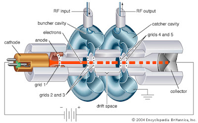
3.Klystrons
Reentrant cavities,Velocity modulation,Bunching,Reflex klystron.

4.Travelling wave tubes 
Slow wave structures,Helix TWT,

5.Magnetrons
Magnetron oscillators (PI mode,Strapping,Mode jumping)

6.Solid state microwave devices
Microwave BJTs,Tunnel Diodes,Gunn Diodes,MESFETs and PIN diodes.

7.Microwave Hybrid Circuits
Magic Tee,Hybrid ring,Directional couplers,Circulators,Isolators.

8.Microwave Measurements
Microwave power,frequency and impedance measurements.


Recommended Standard Texts:

1.Samuel Liao

2.David M Pozar

3.R.E Collin

4.M.Kulkarni [Indian Author]

5.Anapoorna [Indian Author]

Online Materials:

1.MADE EASY class notes

2.PANCEA Class notes

3.IMPATT,BARITT and TRAPATT diodes 

4.Microwave Engineering university questions [Dr APJ Abdul Kalam Technical University]


GATE 2016 Mtech Admission Status

Hi there,

I have secured AIR 103  in GATE ECE 2016.I have lately received queries from many asking me to post about the courses in have applied for.

I have applied for Mtech admission at following IITs.I belong to OBC category.


UPDATE: I have cancelled my offers from IISc and IITB.I have decided to purse a career in VLSI Design by taking M.Tech Microelectronics and VLSI at IIT Madras.

1.IISc Bangalore

My preference order:


  1. Microelectronic Systems
  2. DESE
  3. Communication and Networks
  4. Signal processing


I got offer letter for  Communication and Networks in the first list which was published on April 7th..Also received interview call from DESE.

Fee : Rs. 59,900 to be paid.

Update: I declined the offer for Communication and Networks on MAY 23.
_________________________________________________________________________________

2.IIT Bombay

My preference order:


  1. Microelectronics 
  2. Electronic System Design
  3. Communication Engineering


I got Microelectronics in the first list which was published in April 14th.

Fee : Rs. 28,900 to be paid for confirmation of seat allotted.
_________________________________________________________________________________

3.IIT Madras

I couldn't attend TI sponsored MS test/Interview.

My preference order:


  1. Microelectronics and VLSI Design (EE3Y)
  2. Communication Engineering (EE1Y)


The first list was published on MAY 14 and I got EE1 my second option.I have rejected the offer and requested for upgrade.

Update: I got allotted in Microelectronics and VLSI design  in the second round which was published on 22nd MAY. (Only 14 seats are there.)

Fee: Rs.17,963 to be paid for accept and freeze / accept and upgrade.Also additional hostel fees of Rs.20,150 needs to be paid later.

________________________________________________________________________________

4.IIT Kharagpur

My preference order:

  1. Microelectronics and VLSI
  2. Communication Engineering
  3. Control engineering


The first list came on MAY 2nd.I got my first option there as well.I rejected the offer.
________________________________________________________________________________

5.IIT Delhi

My preference order:


  1. Integrated Electronics and Circuits
  2. VLSI Design Tools and Technology
The cut off scores were 800 ,though I was eligible i could not attend the interview on MAY 17th  & 18th.
 Check out the interview experience of my friend who got selected there.

_________________________________________________________________________________

MY OFFER LETTERS (PROUD and HAPPY  MOMENTs )


IIT BOMBAY 

IISc
IIT MADRAS